Tips for low-cost Electron Beam Lithography
Electron beam lithography (also known as e-beam lithography) is a technique for creating patterns on a substrate by focusing an electron beam. An electron-sensitive layer, also known as a resist, is applied to the surface of the substrate. It does not lay the material on the surface but rather alters the solubility of the resist that is already on the surface. When subjected to an electron beam, the solubility of the resist varies, allowing it to be systematically removed. Depending on the resistance, the revealed part becomes more soluble, while the unexposed section becomes less soluble. The resist may be easily removed by soaking it in a solvent, a process known as ‘developing.’ Small features are produced in the resist, much to photolithography, and then transmitted to a substrate by etching.
The most significant benefit of electron beam technologies over traditional photolithography is creating patterns with nanoscale resolutions. ebeam technology is a maskless technology that has a high resolution but a limited throughput. As a result, its applications are confined to photomask fabrication, low-volume semiconductor device production, and research and development.
Table of Contents
How to save money on E-beam Lithography Systems
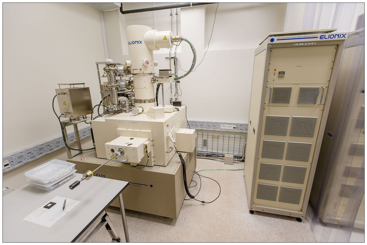
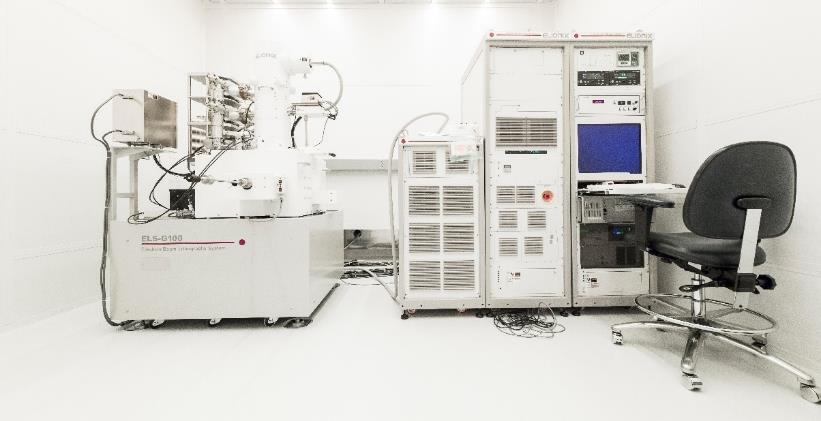
Ion beam lithography systems used for commercial applications are expensive since they are specialized electron beam writing systems (greater than USD One Million). An electron microscope is typically transformed into an e-beam lithography device for research purposes by adding extra equipment that is very affordable (USD 100 K). Although these converted systems do not attain the resolution inherent in e-beam lithography methods, they produce linewidths of 10nm.
The beam shape and the mechanism utilized for beam deflection are used to classify EBL lithography systems. Earlier systems relied on Gaussian-shaped beams to scan the surface. Modern systems use shaped beams that can be vector scanned, which means they may be deflected to numerous points in the writing field.
Electron generators
Electron beam lithography resolution systems employ a thermionic source built of lanthanum hexaboride. Field emission sources, such as heated W/ZrO2 for reduced energy spread and improved brightness, are used to attain high resolutions. Field emission sources are classified into two types: thermal emission sources and cold emission sources. Thermal emission sources have a larger beam size than cold emission sources. On the other hand, thermal field emission sources are typically favored because of their greater stability during lengthy writing durations. Lenses
Electrostatic and magnetic lenses can both be utilized. Electrostatic lenses, on the other hand, are not appropriate for fine focusing due to higher aberration. Because chromatic electron beams are not currently created, fine focusing is accomplished by employing a very tiny dispersion of electron beam energy.
Alignment, Stitching, and Stage
Electrostatic lenses can be utilized for very tiny beam deflections, but electromagnetic lenses are needed for significant beam deflections. The writing field is approximately 100 microns to 1 millimeter due to the inaccuracy and a limited number of steps in the exposure grid. For sketching huge designs, the stage must be altered. Stitching (tiling writing fields against one another) and pattern overlay need precise stage placement (aligning a pattern to the earlier drawn pattern).

Time required for Electron Beam Writing
The shortest amount of time necessary to expose a given area may be represented as D. A = T.
Where I is the beam current, D is the dosage, A is the exposed area, and the item must be exposed for a duration T (which may be further broken into exposure time per unit step size). According to the above calculation, if a 1 cm2 area is treated to a dose of 10-3 C/cm2 at a beam current of 10 nano amperes, the time required to write is 106 s or 12 days. Additional time is required for stage adjustment, blanking the beam (blocking while deflection), and so on. Similarly, it takes around 22 years to cover 700 cm2 of a 300 mm silicon wafer. Therefore, throughput is a major issue in e-beam lithography, and it is exacerbated when generating dense patterns across bigger regions. This effectively rules out any commercial-scale manufacture using this technology.
Because of the tiny field of electron beam used to write the pattern, this electron beam melting process is much slower than ordinary photolithography. Because of the small size of the electron field, multiple exposure fields are required to scan to create a pattern. In contrast, the field size in an e-beam is less than one mm2, yet it is higher than 40 mm2 inside an optical mask projection scanner—furthermore, the stage shifts between field scans. Because of the tiny size, a raster scan is necessary to make patterns (for example, 26 mm × 33 mm pattern) in e-beam, while photolithography requires a one-dimensional scan. An optical maskless lithography tool is currently significantly quicker than an e-beam tool for a given resolution when patterning a photomask.


